
Probe Card
Working in the semiconductor industry it is possible having to develop a test board with specific characteristics and able to adapt at the following DUT (Device Under Test).
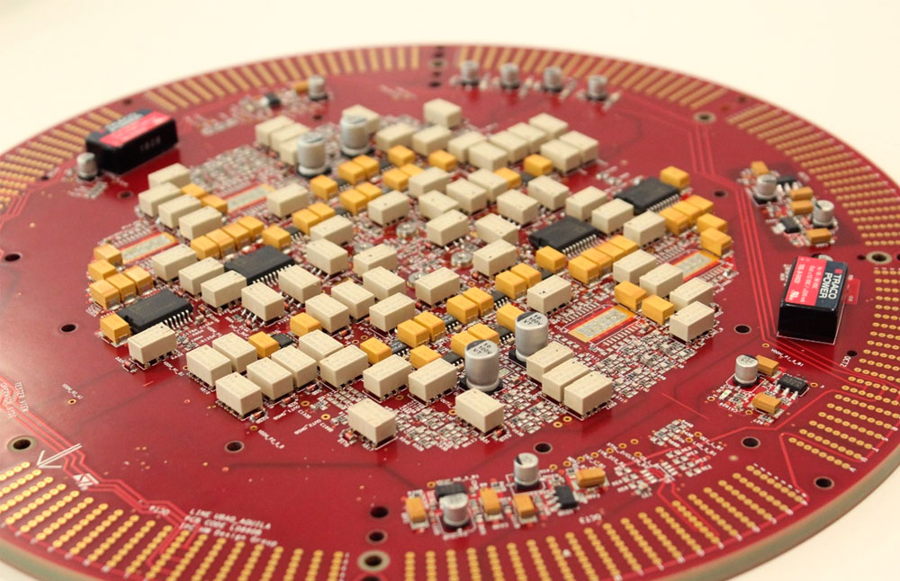
In this case we will talk about a Probe Card, a circular board with 11 inch of diameter (27.94 cm) and an high thickness of 7 mm compared to 1.6 mm standard.
As you can see in the figure 1, the board has a central area, that we call TOP, where the component necessary for a signal conditioning can be positioned. In the external part, where there are no components, there is an area dedicated to contacting the Tester’s pins. The tester is a device able to generate and read mixed signals (analog and digital) and to stimulate the system and test the performances through a specific test program.


Before arriving at the DUT, the signals coming from the device can pass through a conditioning circuit to assume certain performances or different combinations.
The signals coming from the Tester instead are connected to the board through the contact with retractable pins that are based on specific sites on the TOP side of the external part.
On the opposite side of the board, that we call Bottom, are based the DUT through a socket that provides the connection with measuring Resources (signals).

In this case is clear that the value of the electrical measurements, necessary to the functional and the performance characterization of the system, has to be as much indipendent as possible from the board that represents an interface between the tester and the device. The board has to be designed to impact as little as possible on the values of the signals sent and reviewed below.
For example, we are able to realize a board representing some specific lines in a particular section of the conditioning circuit with a low capacitive impact (less than 10 pF).
These lines are closed of DUT and therefore it may represent some difficulties for a board with an high density as the board represented in the figure below..

The capacity of a line on a printed circuit is determined by the geometric characteristics of the Net and the phisical characteristic of the medium in which it is located (see figure)

We can simply describe the phenomena in these terms: when in the Net, made up of a conductive material (copper), is injected a signal, it is generated an electric field that you can pair with a conductor nearby.
In a way the Net interacts with closer conductors. The exent of this interaction is function of the width of the Net W, of the distance from the “coupled” conductor and of the medium that separates them (air, dielectric, etc).

Parameterizing what I said, we can generally have:
![]()
Where:
C= Net capacity
ε = dielectric constant of the medium
W= track width
l= track lenght
h= facing conductor distance.
To get back in the costomer’s requirement, we had to create an emptying area compared to the other conductors around the interested Net (high H) keeping the width W and the lenght L, as low as possible.
This entailed the setting of particular routing rules that kept track of these tree parameters and that verified the respect afterwards.

Thank you for your reading. If you have any questions or comments, write to me: I will be happy to answer to all of you.
Andrea Landonio
- Log in to post comments