SDR (software defined radio)

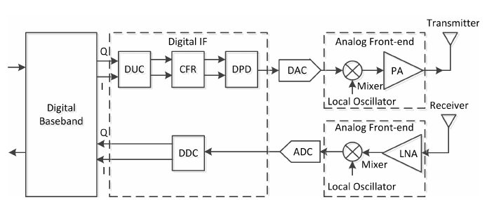
Figure 1 Block diagram of a generical SDR (Software Defined Radio)
In this article we see what is meant by the term "SDR"(Software Defined Radio). This acronym refers to a developing technology that allows to build radio equipment no longer strictly made as pure hardware, but based, or “defined” on software, in particular to manage the modulation and demodulation functions of the signals and, if possible, of hardware configuration. With SRD method you can have a reprogrammable equipment everytime you want to manage a different standard. As we can see at Figure 1, a typical SDR system consists of a series of functional blocks:
Analogic Front-End (RF/IF):
The analogic front-end is the only part of the radio composed by pure hardware. The analog radio frequency signal captured by the antenna is reported in the base band or bandwidth, depending on whether we are in reception or transmission, through the use of an analog mixer. The main specification required for the hardware part is flexibility, which translates to the possibility of changing the carrier frequency of the radio from tens of Mhz to a few Ghz. The hardware chosen is able to change the carrier frequency of the signal in the range from 70 Mhz to 6 Ghz. In order to make everything possible the mixer must be broadband and the local oscillator must be of the voltage controlled type (VCO, Voltage Controlled Oscillator). A band-pass filter can be inserted between the antenna and the mixer but, in order to maintain maximum flexibility, it must have programmable band and central frequency.
Analog/digital conversions and vice versa (ADC - DAC):
Analog-to-digital or digital-to-analog conversion is a mixed block, working on both digital and analog signals, that acts as an interface between the purely hardware part and the part defined via software and then goes to connect the analogue world with the digital world. In order to better understand the operation of this block and its component parts, a distinction must be made between the transmission chain and the receiving chain of a base band signal.
Let’s first analyze the chain of reception of a signal. Digitizing a signal means dividing it into a number of time-balanced samples and associating each sample with a numerical value. These operations are called "sampling" and "quantization" and are carried out within a device called ADC. You will then have to choose an appropriate time interval, called sampling period, and an appropriate number of bits of the quantizer that will then give us the minimum detectable amplitude difference between one sample and the other. For example, if we have 8 bits the minimum voltage difference will be equal to with FS maximum voltage that can be input to the quantizer. The selection of the sampling period
must be done respecting the Sampling Theorem which, imposes a sampling frequency
minimum of two times the signal band
maximum frequency contained in the signal to be sampled. Failure to comply with the constraint will lead to a distortion, by aliasing effect, of the sampled signal spectrum. All components outside the Nyquist range
will recur within the frequency range
In the input to the reception chain you will have as a first step the passage of the analogue signal in the base band through a low pass filter, commonly called anti-aliasing filter, with cut frequency that limits the gang. The filtered signal is then scanned by the Analog/Digital Converter (ADC) and passed to the basic bandwidth processing system. The anti-aliasing filter is an analog filter and as such it has a realization cost that increases with the increase of the order of the filter and therefore with the increase of its filtering capacities. To meet the need for a high-performance hardware that is as economical as possible, downstream of the ADC a rate conversion system called decimator is used. This allows us to use a large fs that translates in terms of sampled signal spectrum with a greater distance between replicates than the minimum fs allowed. The greater the distance between the replicates, the smaller the anti-aliasing filter order. The decimator therefore serves to lower the frequency with which the samples are presented to the processor thus avoiding to increase the computational cost. A generic decimator consists of a low-pass FIR filter operating at the highest rate fs with a cutting frequency equal to half of the lowest rate
Output from the filter is a circuit that resamples the signal at the sample rate fs .
The chain in transmission, unlike the one in reception, takes in a digital base band signal. Digital signal samples enter, with frequency fs in a rate conversion system which performs an over-sampling and interpolation operation. The over-sampling operation is to insert zero-amplitude samples L from one low-rate sample to another. The interpolator FIR filter, which is a low pass filter operating at high rates fs with cutting frequency shall assign a numerical value to the added samples between one low-rate sample and the next. The ultimate goal in using this technique is also the possibility to use an anti-image filter output from the DAC (Analog Digital Converter) as simple and economical as possible. An anti-image filter is a low-pass filter that smoothes out the step response of the DAC.
BBP (Processing in basic band):
Last block, but not least, of the SDR system is the BBP in which the digital signal in the base band is generated or processed. Generally, given the amount of data that the device is to manage and given the requirements of flexibility and reprogramming that it must comply, the block is realized through FPGA technology that allows the realization of coProcessors capable of running parallel operations. Large amounts of data can be processed very quickly and thus a lower clock rate can be allowed than a microprocessor-based system that performs sequential operations. It therefore has full control over the power consumption that is generally a basic requirement in the space but even more important within a Cubesat.
- Log in to post comments